NVIDIA Blackwell vs AMD MI350: The AI Accelerators Defining the Infrastructure Race
These are not consumer GPUs. They are purpose-built compute racks designed to train and serve large language models at a scale that would have been supercomputing-class just five years ago. Understanding how they differ is no longer an academic exercise. It is an infrastructure buying decision.
Every frontier AI model that ships today runs on infrastructure most people never see. Beneath the chat interface and the API call sits a data center floor humming with specialized silicon — and in 2026, two platforms dominate that conversation: NVIDIA's Blackwell GB200 and AMD's Instinct MI350.
These are not consumer GPUs. They are purpose-built compute racks designed to train and serve large language models at a scale that would have been supercomputing-class just five years ago. Understanding how they differ is no longer an academic exercise. It is an infrastructure buying decision.
This article breaks down the architectural differences, benchmark realities, ecosystem trade-offs, and practical guidance for teams choosing a platform in 2026.
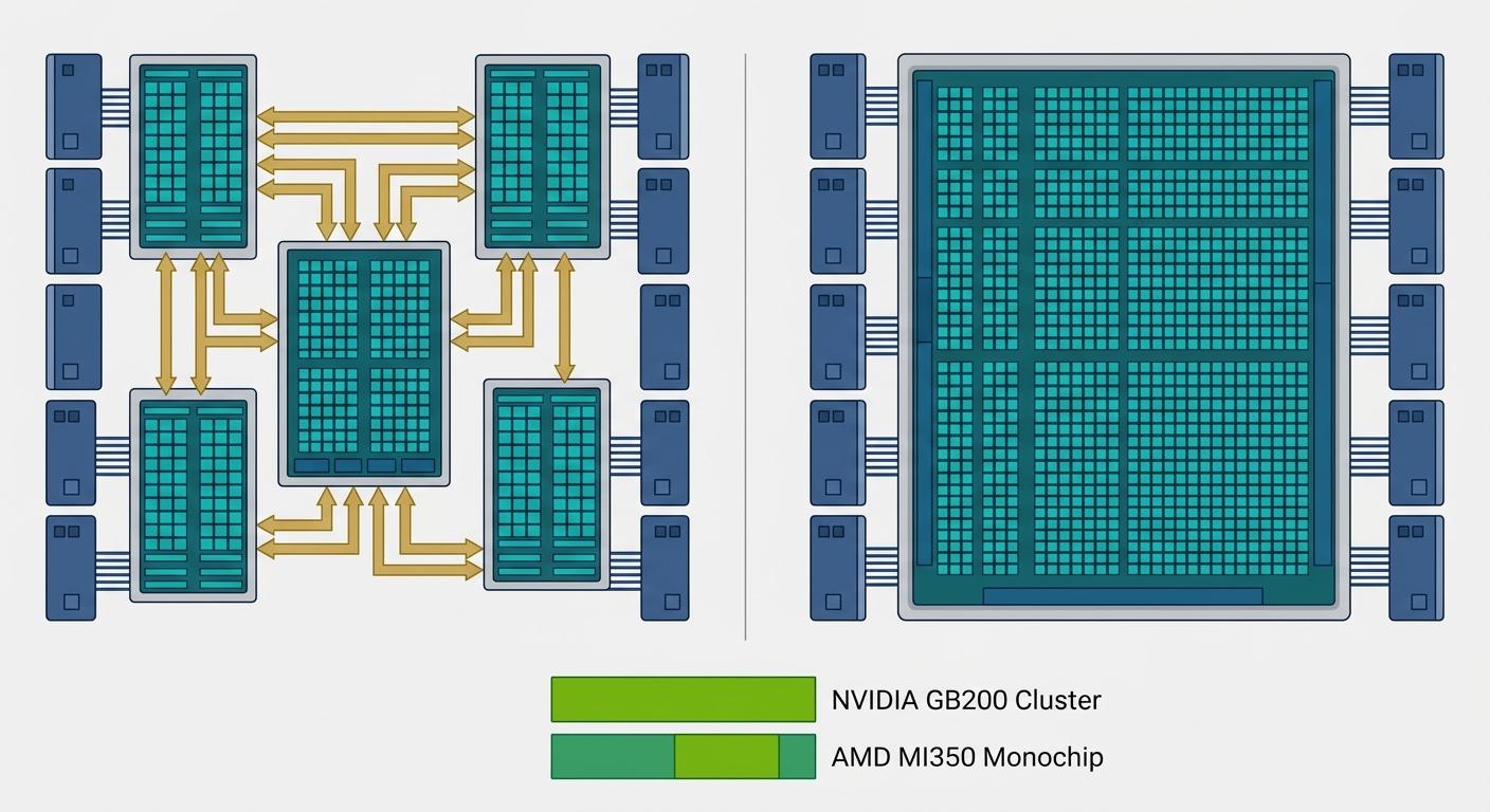
How the Two Architectures Stack Up
At the silicon level, Blackwell and MI350 take meaningfully different approaches to solving the same problem: moving enormous amounts of data through matrix multiplication as efficiently as possible.
NVIDIA Blackwell GB200 uses a 2-die configuration built on TSMC's 4NP process. The architecture houses 208 billion transistors across two compute dies connected to a separate GPU die, all sharing access to 192GB of HBM3e memory per GPU at approximately 8 TB/s of bandwidth. A defining feature is the Transformer Engine — a dedicated hardware block that dynamically adjusts precision (FP16, BF16, FP8) per layer during LLM inference and training. This gives Blackwell a structural advantage on transformer-based workloads without requiring code changes.
AMD MI350 uses the CDNA 4 architecture on a combination of TSMC 5nm and 6nm processes. It is designed as a monolithic die approach with 288GB of HBM4 memory per GPU at approximately 6.5 TB/s bandwidth. AMD's equivalent compute units are called AI Matrix Cores (their branding for the CDNA-generation tensor units). The architecture also includes AI STRETCH instructions — specialized vector-matrix operations designed to accelerate specific inference kernels.
The memory story is one of the clearest differentiators. MI350's 288GB per GPU substantially exceeds Blackwell's 192GB. For teams running large model checkpoints that do not fit cleanly into a single GPU's VRAM, this capacity advantage reduces the complexity of model-parallel sharding.
Performance: Training and Inference at Scale
Raw performance comparisons in AI hardware are complicated by workload dependence. Different models, batch sizes, and precision modes produce different rankings. That said, some patterns are consistent enough to guide decisions.
Inference performance is where Blackwell draws the most attention. NVIDIA's own benchmarks show approximately 2.5x improvement in tokens-per-second-per-GPU for LLM inference workloads compared to the H100 generation. (External validation from MLCommons and third-party reviewers is still accumulating as of mid-2026.) The mechanism is straightforward: the Transformer Engine eliminates precision bottlenecks in attention computation, and NVLink 5.0 keeps data flowing between GPUs without hitting PCIe bandwidth ceilings.
AMD's MI350 delivers roughly 1.4x improvement over the MI300X generation in FP16 and FP8 throughput, based on AMD's published performance data. For teams already on AMD infrastructure, this is a meaningful step forward. The MI350 also improves on memory-bound inference scenarios due to its larger HBM4 capacity, which reduces the frequency of weight swapping for models that previously required multi-GPU tensor parallelism.
Training performance is more balanced. Both platforms handle large-scale distributed training across hundreds of GPUs in multi-node configurations. Blackwell's NVLink 5.0 provides 1.8 TB/s intra-rack bandwidth — significantly faster than the PCIe generational path and a meaningful advantage for data-parallel and model-parallel training alike. MI350 uses Infinity Fabric Link to connect multiple GPUs, achieving multi-node scaling that AMD positions as competitive for mainstream LLM training workloads (up to approximately 70B–130B parameter models at reasonable batch sizes).
Realistic expectation — For teams running 8-GPU or 16-GPU training jobs, performance differences between the platforms are likely smaller than the ecosystem and infrastructure differences that accompany them.
Memory: Capacity vs Bandwidth Trade-Off
The GB200 versus MI350 memory profiles reflect two different design philosophies.
| Specification | NVIDIA GB200 | AMD MI350 |
|---|---|---|
| Memory per GPU | 192GB HBM3e | 288GB HBM4 |
| Peak Bandwidth | ~8 TB/s | ~6.5 TB/s |
| Memory Capacity (8-GPU node) | 1.5TB | 2.3TB |
| FP8 Support | Yes, native | Yes, native |
Bandwidth-bound workloads — such as autoregressive inference at high batch sizes — favor GB200's 8 TB/s. The transformer attention mechanism is memory-bandwidth intensive, and Blackwell's wider bus translates directly to higher throughput per token generated.
Capacity-bound workloads — such as serving a 400B parameter model in full precision on a single node — favor MI350's 288GB. Fitting the entire model in one GPU eliminates the overhead of tensor parallelism for certain deployment scenarios, which can reduce latency and simplify serving stack complexity.
For sovereign AI deployments where multi-node interconnect bandwidth may be limited, MI350's capacity advantage is frequently decisive. Keeping the full model on one node avoids the latency and bandwidth overhead of cross-node communication.
The Software Battle: CUDA vs ROCm
Hardware performance only materializes through software. This is where the gap between NVIDIA and AMD remains most pronounced.
NVIDIA's CUDA ecosystem is 15+ years old. The stack includes cuDNN for deep learning primitives, TensorRT for inference optimization, Triton Inference Server for serving, and cuQuantum for quantum circuit simulation. Every major ML framework — PyTorch, JAX, TensorFlow — has CUDA as its primary optimization target. For infrastructure teams, this means: most models work, most optimizations are available, and most engineers already know the toolchain.
AMD's ROCm stack has improved dramatically. ROCm 6.x includes native PyTorch 2.0+ support, improved TensorFlow compatibility, and a CUDA compatibility layer that allows some existing codebases to run without modification. However, the ecosystem is still materially smaller. Some third-party libraries, inference engines, and cloud-native tools have incomplete or delayed ROCm ports.
The practical implication is not that AMD is unusable — many production deployments run successfully on MI300X and MI350 — but that migration and debugging costs are higher when unexpected compatibility issues arise. Teams evaluating AMD should budget explicit time for ROCm validation of their specific model serving stack.
The ecosystem gap is narrowing. AMD's investments in ROCm and acquisitions (including Silo AI in late 2025) mean the trajectory favors gradual convergence. But in 2026, CUDA remains the lower-risk choice for teams without existing AMD expertise.
Power, Cooling, and Rack Density
Infrastructure planners cannot ignore the physical reality of these systems.
GB200's power density is the most cited challenge. A fully configured Blackwell rack can consume over 100kW — roughly 2–3x the power density of an H100 rack. This is not a marginal difference. It requires liquid cooling (direct liquid cooling or rear-door heat exchangers), data center power infrastructure upgrades, and raised floor reinforcement in many facility designs.
MI350's power envelope is more tractable. At approximately 70kW per rack, it fits more comfortably within existing data center designs, especially facilities built within the last five years that anticipated GPU density increases.
For hyperscalers building greenfield facilities, Blackwell's density is an engineering problem with known solutions. For enterprise teams retrofitting existing data centers, MI350's power profile may be the deciding factor — the cost of electrical and cooling upgrades can easily exceed the hardware cost differential.
Market Reality: Who's Buying What in 2026
The deployment landscape reflects both technical merit and business relationships.
NVIDIA Blackwell is already available in Google Cloud (GB200 A3 VMs), Oracle Cloud Infrastructure, and select Lambda Labs configurations. Microsoft Azure has announced Blackwell integration for its HPC and AI workloads. Broad enterprise availability shifted toward Q3 2026 as NVIDIA manages allocation against enormous demand.
AMD MI350 shipped to select hyperscalers in Q1 2026, with broader enterprise availability through OEM channels in Q2 2026. AMD has positioned MI350 explicitly as the more available alternative — a deliberate contrast to NVIDIA's constrained supply chain.
Analyst estimates from IDC and Gartner (as of Q1 2026) place NVIDIA at approximately 80% of AI accelerator market share by revenue. AMD holds roughly 15–18%, with Intel and custom silicon (Google TPUs, Amazon Trainium) making up the remainder. MI350's trajectory is upward, but NVIDIA's installed base and developer ecosystem create meaningful inertia.
Which Accelerator Is Right for Your Workload?
No single platform wins universally. The right choice depends on three factors: your existing infrastructure, your workload profile, and your team's expertise.
| Use Case | Recommended | Primary Reason |
|---|---|---|
| Large model training (1T+ parameters) | NVIDIA GB200 | NVLink ecosystem, bandwidth, Transformer Engine |
| Inference serving at scale | NVIDIA GB200 | Per-GPU throughput, mature serving stack (Triton) |
| Large model on-premise (≤8 GPUs) | AMD MI350 | Higher memory capacity, simpler rack requirements |
| Mixed CUDA/ROCm environment | AMD MI350 | ROCm openness, lower hardware cost per node |
| Greenfield hyperscale cluster | NVIDIA GB200 | Ecosystem maturity, highest raw performance |
| Brownfield data center retrofit | AMD MI350 | Lower power density, easier integration |
For most enterprises already running NVIDIA infrastructure, the migration cost to AMD is rarely justified by the performance delta. For new deployments with no existing CUDA investment, MI350 deserves serious evaluation — particularly for capacity-sensitive workloads where the 288GB memory advantage is decisive.
The most important factor is benchmarking your actual workload. Vendor benchmarks are conducted under specific conditions that rarely match production environments exactly. Run your model, your batch size, your precision mode, and measure.
Conclusion
The 2026 AI accelerator race is not a zero-sum outcome. NVIDIA Blackwell leads on raw inference performance and ecosystem depth. AMD MI350 leads on memory capacity and infrastructure accessibility. Both platforms are genuine options for serious AI workloads — a meaningful change from even two years ago when the choice was largely predetermined.
Infrastructure teams should approach this as a systems engineering decision, not a spec sheet comparison. Power infrastructure, cooling capacity, existing software investments, team expertise, and workload characteristics all factor into the right answer.
Start with a benchmark. Match it against your facility constraints. Then decide — because in AI infrastructure, the most expensive mistake is not choosing the wrong chip. It is choosing based on marketing rather than measurement.
Expert Q&A
Q1: How much faster is GB200 compared to H100 for LLM inference?
A: NVIDIA's published figures show approximately 2.5x improvement in tokens-per-second-per-GPU for LLM inference on GB200 versus H100. This is driven by three factors: the dedicated Transformer Engine's FP8 acceleration for attention layers, NVLink 5.0's 1.8 TB/s intra-rack bandwidth (eliminating PCIe bottlenecks in multi-GPU serving), and increased HBM3e memory bandwidth (~8 TB/s vs H100's ~3.35 TB/s).
It is worth noting that NVIDIA's figures represent best-case scenarios on their reference workloads. Third-party validation from MLCommons is ongoing as of mid-2026.
Q2: Does AMD MI350 support FP8 natively?
A: Yes — MI350 supports FP8 natively through its AI Matrix Cores with CDNA 4 architecture. Direct FP8 performance comparisons between MI350 and GB200 are complicated by the lack of standardized third-party benchmarks as of mid-2026.
Q3: Can I run NVIDIA-optimized models on AMD MI350?
A: Most models trained on CUDA can run on AMD MI350 through ROCm. PyTorch 2.0+ has native ROCm support, and the CUDA compatibility layer in ROCm 6.x provides binary-level translation for many kernels. However, TensorRT models cannot run directly — they must be reconverted. The practical migration path for an existing NVIDIA deployment to AMD typically takes 2–6 weeks of engineering time.
Q4: What are the real power and cooling challenges with deploying Blackwell?
A: A single GB200 rack can draw over 100kW under full load. Liquid cooling is mandatory, not optional. For enterprises retrofitting existing data centers, infrastructure costs can add 20–40% to total deployment cost — often overlooked in hardware purchase decisions.
Q5: Which cloud providers offer Blackwell and MI350 instances?
A: As of mid-2026: Google Cloud and Oracle offer GB200 A3 VMs; Lambda Labs has GB200 on-demand instances; Microsoft Azure is rolling out Blackwell through Q3 2026. AWS and Azure offer AMD MI350 (Azure available now; AWS MI350 expected Q3 2026).
Q6: What does the 288GB vs 192GB memory difference mean in practice?
A: For models between 70B–400B in FP16, MI350's 288GB reduces the number of GPUs needed for tensor parallelism versus GB200. For 70B class models specifically, MI350 can fit the full model plus KV cache in a single GPU at batch sizes where GB200 would need 2 GPUs — a meaningful latency and cost advantage.
Next Steps:
- Download our AI Infrastructure Readiness Checklist for data center evaluation
- Compare TCO models for Blackwell vs MI350 deployments with our interactive tool
- Subscribe to the Algorithmine infrastructure newsletter for monthly hardware market analysis
Image URLs
| # | Alt | URL |
|---|---|---|
| 1 | Side-by-side architectural block diagram comparing NVIDIA GB200 multi-die design with two compute dies connected via NVLink, and AMD MI350 monochip design | /api/images/e4df0c441d254990a55ceb050db59c67 |
Total: 1 image uploaded